The quality indicators for evaluating switch mode power supplies should prioritize safety and reliability. Under the condition that the electrical technical indicators meet the requirements for normal use, in order to ensure the safe and reliable operation of the power supply in harsh environments and sudden faults, it is necessary to design various protection circuits, such as anti surge soft start, anti overvoltage, undervoltage, overheating, overcurrent, short circuit, and phase loss protection circuits. At the same time, in the same switching power supply circuit, the interrelated design of multiple protection circuits and the issues to be noted should also be given sufficient attention.
1.Anti surge soft start circuit
The input circuit of switch mode power supplies mostly adopts capacitor filtering rectifier circuits. At the moment of closing the incoming power supply, due to the initial voltage on the capacitor being zero, a large surge current will be formed during the charging of the capacitor. Especially for high-power switch mode power supplies, larger filtering capacitors are used to make the surge current reach over 100A. At the moment of power connection, such a large surge current can often cause the input fuse to burn out or the contact of the closing switch to burn out, and the rectifier bridge to be damaged due to overcurrent; Even light ones can cause the air switch to fail to close. The above phenomena can cause switching power supplies to malfunction. Therefore, almost all switching power supplies are equipped with soft start circuits to prevent surge currents to ensure the normal and reliable operation of the power supply. Anti surge soft start circuits usually have two categories: thyristor protection method and relay protection method.
(1) Thyristor protection method
Figure 1 shows an anti surge current circuit composed of a thyristor V and a current limiting resistor R1. At the moment of power connection, the input voltage charges capacitor C through the rectifier bridge (D1~D4) and the current limiting resistor R1, limiting the surge current. When capacitor C is charged to about 80% of the rated voltage, the inverter operates normally. The triggering signal of the thyristor is generated by the auxiliary winding of the main transformer, causing the thyristor to conduct and short-circuit the current limiting resistor R1, and the switching power supply is in normal operation.
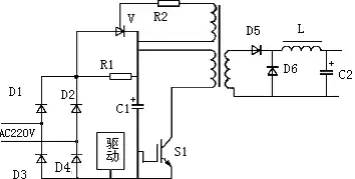
Figure 1: Anti surge current circuit composed of thyristors and current limiting resistors
(2) Relay protection method
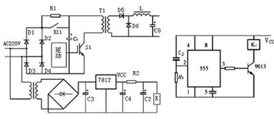
Figure 2: Anti surge current circuit composed of relay K and current limiting resistor R1. Figure 3: Replacing R2C2 delay circuit
Figure 2 shows an anti surge current circuit composed of relay K and current limiting resistor R1. At the moment of power connection, the input voltage is rectified (D1~D4) and the limiting resistor R1 charges the filtering capacitor C1 to prevent surge current at the moment of connection. At the same time, the auxiliary power supply Vcc charges the capacitor C2 connected to the relay K line package through resistor R2. When the voltage on C2 reaches the operating voltage of relay K, K acts, and its contact K1.1 closes, bypassing the limiting resistor R1, and the power supply enters normal operation state. The delay time of current limiting depends on the time constant (R2C2), usually selected between 0.3 and 0.5 seconds. In order to improve the accuracy of delay time and prevent relay action jitter and oscillation, the delay circuit can replace the R2C2 delay circuit with the circuit shown in Figure 3.
2.Overvoltage, undervoltage, and overheating protection circuits
The harm caused by overvoltage and undervoltage of the incoming power supply to the switching power supply is mainly manifested in the damage of devices due to the voltage and current capacity they bear exceeding the normal range of use, and the inability to meet the requirements due to the destruction of electrical performance indicators. Therefore, there should be limitations on the upper and lower limits of the input power supply, and overvoltage and undervoltage protection should be adopted to improve the reliability and safety of the power supply.
Temperature is the most important factor affecting the reliability of power supply equipment. According to relevant data analysis [5], for every 2 ℃ increase in temperature of electronic components, reliability decreases by 10%. The working life at a temperature rise of 50 ℃ is only 1/6 of that at a temperature rise of 25 ℃. In order to avoid damage caused by overheating of power devices, an overheating protection circuit is also required in switch mode power supplies.
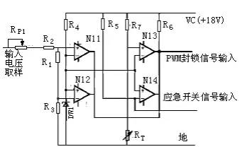
Figure 4 Overvoltage, undervoltage, and overheat protection circuit
Figure 4 shows an overvoltage, undervoltage, and overheating protection circuit composed solely of a 4-comparator LM339 and several discrete components. The sampling voltage can be directly obtained from the auxiliary control power supply after rectification and filtering, which reflects the changes in input power supply voltage. The comparator shares a common reference voltage, with N1.1 being the undervoltage comparator and N1.2 being the overvoltage comparator. Adjusting R1 can adjust the action thresholds of overvoltage and undervoltage. N1.3 is an overheat comparator, and RT is a thermistor with negative temperature coefficient. It forms a voltage divider with R7 and is closely attached to the surface of the power switching device IGBT. As the temperature increases, the resistance value of RT decreases. Properly select the resistance value of R7 to activate N1.3 at the set temperature threshold. N1.4 is used for emergency shutdown of external faults. When its forward end input is low, the comparator outputs a low-level blocking PWM drive signal. Due to the parallel connection of the output terminals of the four comparators, regardless of any fault such as overvoltage, undervoltage, or overheating, the comparator outputs a low level and blocks the drive signal to stop the power supply from working, achieving protection. If the circuit is slightly modified, the comparator can also output a high-level blocking drive signal.
3.phase loss protection circuit
Due to the inherent reasons of the power grid or unreliable power input wiring, switch mode power supplies may sometimes experience phase loss operation, which is difficult to detect in a timely manner. When the power supply is in phase loss operation, one arm of the rectifier bridge has no current, while the other arms will be severely overcurrent causing damage and causing abnormal operation of the inverter. Therefore, it is necessary to protect the phase loss. Current transformers or electronic phase loss detection circuits are commonly used to detect phase loss in the power grid. Due to the high cost and large volume of current transformer detection, electronic phase loss protection circuits are generally used in switching power supplies. Figure 5 is a simple phase loss protection circuit. When three-phase balance is achieved, the H potential at nodes R1 to R3 is very low, and the optocoupler output is approximately zero level. When there is a phase loss, the H-point potential rises, and the optocoupler outputs a high level. After comparison by a comparator, it outputs a low level and blocks the driving signal. The benchmark of the comparator is adjustable to adjust the threshold of phase loss action. This phase loss protection is applicable to three-phase four wire systems, but not to three-phase three wire systems. The circuit can be slightly modified, and high-level blocking of PWM signals can also be used.
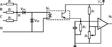
Figure 5 Phase loss protection circuit for three-phase four wire system
Figure 6 is a phase loss protection circuit for three-phase three wire power supplies. If any phase A, B, or C is missing, the output level of the optocoupler is lower than the reference voltage of the inverter input terminal of the comparator. The comparator outputs a low level, blocks the PWM drive signal, and turns off the power. The input polarity of the comparator can be slightly changed, and a high-level blocking PWM signal can also be used. This phase loss protection circuit uses optocouplers to isolate strong electricity, which is safe and reliable. RP1 and RP2 are used to adjust the threshold of phase loss protection action.
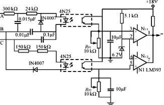
Figure 6 Phase loss protection circuit for three-phase three wire system
4.Short circuit protection
Like other electronic devices, short circuit is the most serious fault in switch mode power supplies. The reliability of short circuit protection is an important factor affecting the reliability of switch mode power supplies. IGBT (Insulated Gate Bipolar Transistor) combines the characteristics of high input impedance, low driving power, high voltage and current capacity, and reduced transistor voltage of field-effect transistors. It is currently the most commonly used power electronic switching device in medium and high-power switching power supplies. The short-circuit time that IGBT can withstand depends on its saturation voltage drop and short-circuit current, usually only a few μ S to several tens μ S. Excessive short-circuit current not only shortens the short-circuit withstand time, but also causes a significant decrease in current during shutdown. Due to the presence of leakage inductance and lead inductance, the IGBT collector overvoltage occurs, which can cause IGBT locking to fail. At the same time, high overvoltage can cause IGBT breakdown. Therefore, effective protective measures must be taken when a short circuit or overcurrent occurs.
In order to achieve short-circuit protection of IGBT, overcurrent detection must be carried out. The method suitable for IGBT overcurrent detection usually uses a Hall current sensor to directly detect the current Ic of the IGBT, and then compares it with the set threshold, using the output of the comparator to control the turn off of the driving signal; Alternatively, the indirect voltage method can be used to detect the voltage drop Vce of the IGBT during overcurrent, as the voltage drop of the transistor contains information about short-circuit current. During overcurrent, Vce increases and is basically linear. The Vce during overcurrent is detected and compared with the set threshold, and the output of the comparator controls the shutdown of the driving circuit.
When a short circuit current occurs, in order to avoid overvoltage caused by excessive turn off current, which may result in ineffective and damaged IGBT locking, and to reduce electromagnetic interference, soft gate voltage reduction and soft turn off comprehensive protection technology are usually used.
When designing a gate voltage drop protection circuit, it is important to choose the correct gate voltage drop amplitude and speed. If the gate voltage drop amplitude is large (such as 7.5V), the gate voltage drop speed should not be too fast. Generally, 2 can be used μ The soft gate voltage reduction with a decrease time of s, due to the large amplitude of the gate voltage reduction, the collector current is already small. In the fault state, the gate can be locked faster without the need for soft shutdown; If the amplitude of gate voltage reduction is small (such as below 5V), the gate voltage reduction speed can be faster, while the speed of gate voltage blocking must be slow, that is, soft shutdown is used to avoid overvoltage.
In order to ensure uninterrupted operation of the power supply in the short circuit fault state and avoid thermal accumulation caused by continuous short circuit protection at the original working frequency, the use of gate voltage reduction protection can eliminate the need to immediately block the circuit in a short circuit protection, and reduce the working frequency (such as about 1Hz), forming an intermittent "hiccup" protection method. After the fault is eliminated, normal operation is restored. The following are several practical circuits and working principles for IGBT short circuit protection.
(1) Design overcurrent protection circuit using Vce of IGBT
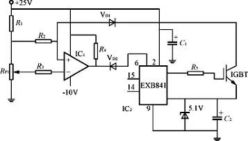
Figure 7: Protection using the principle of increasing Vce when IGBT overcurrent occurs
Figure 7 is a circuit that utilizes the principle of increasing Vce during IGBT overcurrent for protection, used for the dedicated driver EXB841. The internal circuit of EXB841 can effectively perform gate reduction and soft shutdown, and has internal delay function to eliminate false actions caused by interference. The Vce containing IGBT overcurrent information is not directly sent to the collector voltage monitoring pin 6 of EXB841. Instead, it is quickly restored through diode VD1 and output to pin 6 of EXB841 through comparator IC1. The purpose is to eliminate the difference in forward voltage drop of VD1 with different currents. A threshold comparator is used to improve the accuracy of current detection. If overcurrent occurs, the low-speed cut-off circuit of driver EXB841 slowly shuts off the IGBT to avoid damage to the IGBT device caused by the spike pulse of the collector current.
(2) Design overcurrent protection circuit using current sensors
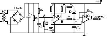
(a) Using current sensors for overcurrent protection circuits

(b) Output driving waveform diagram of PWM control circuit
Figure 8 Using current sensors for overcurrent protection
Figure 8 (a) shows an IGBT protection circuit that uses a current sensor for overcurrent detection. The primary (1 turn) of the current sensor (SC) is connected in series in the collector circuit of the IGBT. The overcurrent signal induced by the secondary is rectified and sent to the same phase input terminal of comparator IC1, which is compared with the reference voltage of the reverse phase terminal. The output of IC1 is sent to comparator IC2 with positive feedback, which is connected to the output control pin 10 of PWM controller UC3525. However, when the current is flowing, VAVref and VB are at a high level. C3 charging makes VC>Vref, and IC2 outputs a high level (greater than 1.4V), closing the PWM control circuit. Due to the lack of driving signal, the IGBT is turned off, and the power supply stops working. The current sensor has no current flowing, causing the VA parameter to turn off the PWM driving signal for t2>>t1, which can ensure that the power supply enters a sleep state. The positive feedback resistor R7 ensures that IC2 only has two states: high and low. The D5, R1, and C3 charging and discharging circuits ensure that the output of IC2 does not frequently change between high and low levels, that is, the IGBT does not frequently turn on or off and be damaged.
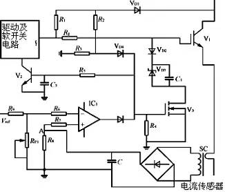
(3) Integrated overcurrent protection circuit
Figure 9 is a comprehensive protection circuit that utilizes IGBT (V1) overcurrent collector voltage detection and current sensor detection. The working principle of the circuit is that when the load is short circuited (or IGBT is overcurrent due to other faults), the Vce of V1 increases, and the V3 gate driving current passes through R2. The R3 voltage divider makes V3 conductive, and the IGBT gate voltage is reduced by VD3, limiting the amplitude of the IGBT peak current. At the same time, it is delayed by R5C3 to make V2 conductive, sending a soft turn off signal. On the other hand, during a short circuit, the current sensor detects the short-circuit current, and the high level output by comparator IC1 causes V3 to conduct for gate voltage reduction, while V2 conducts for soft shutdown.
In addition, the overcurrent protection principle for detecting IGBT collector voltage can also be applied, using short-circuit protection circuits with soft gate voltage reduction, soft turn off, and reduced operating frequency protection techniques [7, 8]. We will not provide a detailed introduction here. Interested readers can refer to reference [1]. Although the protection function of switch mode power supply is an additional function required for the electrical performance of the power supply device, it is crucial for the safety and reliability of the power supply device to ensure that the protection circuit is complete and operates according to the predetermined settings in harsh environments and accident conditions. When accepting technical indicators, the protection function should be verified.
The protection schemes and circuit structures of switch mode power supplies have diversity, but for specific power supply devices, a reasonable protection scheme and circuit structure should be selected to truly and effectively achieve protection under fault conditions.
5.Conclusion
Although the protection function of switch mode power supply is an additional function required for the electrical performance of the power supply device, it is crucial for the safety and reliability of the power supply device to ensure that the protection circuit is complete and operates according to the predetermined settings in harsh environments and accident conditions. When accepting technical indicators, the protection function should be verified.
The protection schemes and circuit structures of switch mode power supplies have diversity, but for specific power supply devices, a reasonable protection scheme and circuit structure should be selected to truly and effectively achieve protection under fault conditions.
After the design of the switch power supply protection circuit is completed, it is necessary to conduct aging experiments on the switch power supply before verifying the functions of various protection circuits.


